Have a question
Or need a free quote?
Click Here to Contact Us
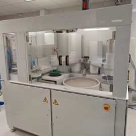
Single/Double Side CMP & Polishing Services
Capabilities:
Utilising Optim Wafer Services’ unrivalled wafer polishing skills, we are able to polish or CMP the following materials.
- Silicon, SiO2, SiGe, Ge, GaN, Glass, Fibre Glass & Sapphire.
- Removal Rates – Low or High removal rates as required.
- Low Surface Roughness – Typical Ra of <1nm.
- Volumes – Large or Small we can manage either.
Typical requests for this type of service require high precision in terms of the control of the material to be removed. Some requests require us to CMP only 1-2µ of material. The typical applications for this wafer CMP service include:
- Preparation for layer transfer.
- EPI Ready surfaces.
- Roughness reduction for Boncing or TSV applications.
- Oxide Planarisation.
Double Side Polishing
Optim Wafer Services is able to offer additional Double side polishing of substrates for the following types of applications:
- Post-thinning of substrates that are required to be a nonstandard thickness.
- To open Poly filled TSV’s but leave a clean, mirror polished surface.
- Post-thinning of an SOI wafer or Bonded pair of wafers.
Typically we are able to achieve low Ra with Semi Standard levels of Metallics and Defects.
Our Other Wafer Processing Services